- 您现在的位置:买卖IC网 > Sheet目录1904 > AT91SAM9G20B-CFU (Atmel)IC MCU ARM9 247-LFBGA
6
6384DS–ATARM–13-Jan-10
AT91SAM9G20 Summary
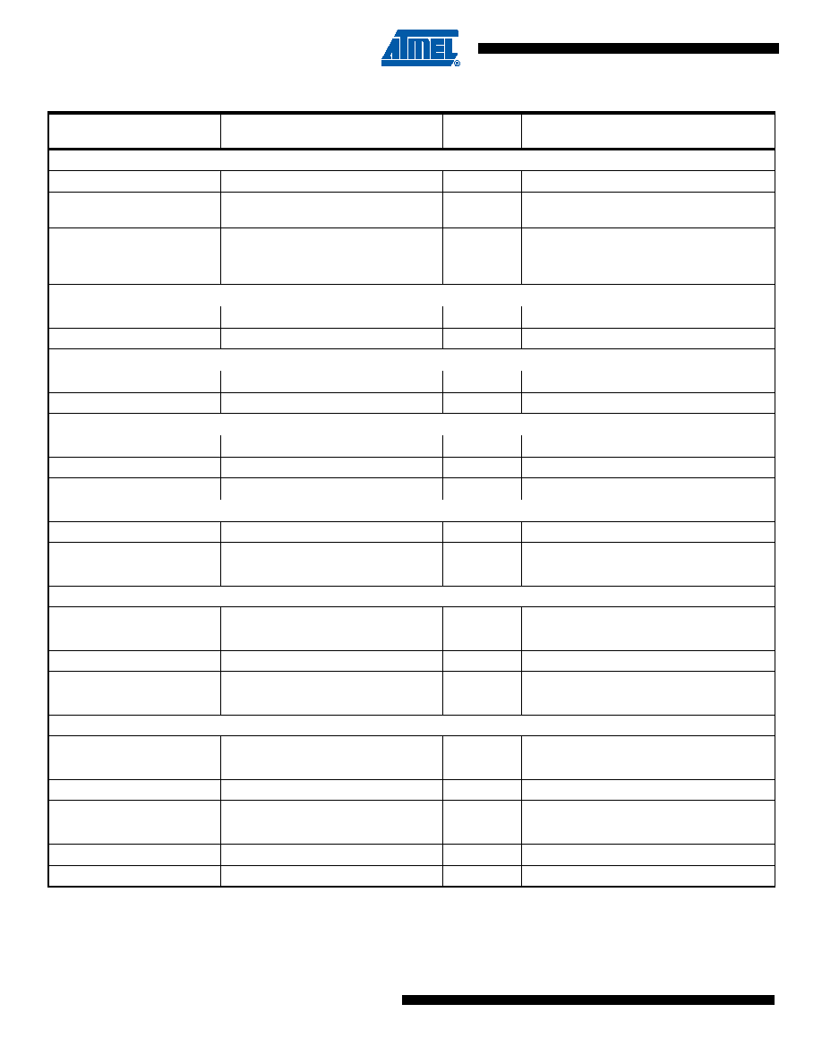
Reset/Test
NRST
Microcontroller Reset
I/O
Low
Pull-up resistor
TST
Test Mode Select
Input
Pull-down resistor. Accepts
between 0V and VDDBU.
BMS
Boot Mode Select
Input
No pull-up resistor
BMS = 0 when tied to GND.
BMS = 1 when tied to VDDIOP.
Debug Unit - DBGU
DRXD
Debug Receive Data
Input
DTXD
Debug Transmit Data
Output
Advanced Interrupt Controller - AIC
IRQ0 - IRQ2
External Interrupt Inputs
Input
FIQ
Fast Interrupt Input
Input
PIO Controller - PIOA - PIOB - PIOC
PA0 - PA31
Parallel IO Controller A
I/O
Pulled-up input at reset
PB0 - PB31
Parallel IO Controller B
I/O
Pulled-up input at reset
PC0 - PC31
Parallel IO Controller C
I/O
Pulled-up input at reset
External Bus Interface - EBI
D0 - D31
Data Bus
I/O
Pulled-up input at reset
A0 - A25
Address Bus
Output
0 at reset
NWAIT
External Wait Signal
Input
Low
Static Memory Controller - SMC
NCS0 - NCS7
Chip Select Lines
Output
Low
NWR0 - NWR3
Write Signal
Output
Low
NRD
Read Signal
Output
Low
NWE
Write Enable
Output
Low
NBS0 - NBS3
Byte Mask Signal
Output
Low
CompactFlash Support
CFCE1 - CFCE2
CompactFlash Chip Enable
Output
Low
CFOE
CompactFlash Output Enable
Output
Low
CFWE
CompactFlash Write Enable
Output
Low
CFIOR
CompactFlash IO Read
Output
Low
CFIOW
CompactFlash IO Write
Output
Low
CFRNW
CompactFlash Read Not Write
Output
CFCS0 - CFCS1
CompactFlash Chip Select Lines
Output
Low
Table 3-1.
Signal Description List (Continued)
Signal Name
Function
Type
Active
Level
Comments
发布紧急采购,3分钟左右您将得到回复。
相关PDF资料
AT91SAM9N12-CU
IC MCU ARM9 217-LFBGA
AT91SAM9R64-CU-999
IC MCU ARM9 32KB ROM 144LFBGA
AT91SAM9XE512-QU
MCU ARM9 512K FLASH 208-PQFP
AT97SC3204-X1A50-1
CRYPTO TPM LPC 3.0-3.6V 28TSSOP
ATA6620N-TAQY
TXRX LIN BUS W/VREG SO-8
ATA6661-TAQJ 19
TXRX LIN 2.0 3.3V/5V 8SOIC
ATA6670-FFQW
IC TXRX LIN DUAL 14VDFN
ATAM893T-TKSYD
IC MCU FLASH 4K MTP 20SSOP
相关代理商/技术参数
AT91SAM9G20B-CU
功能描述:ARM微控制器 - MCU 2x16K SRAM Ethernet USB Host Bus Intrfc
RoHS:否 制造商:STMicroelectronics 核心:ARM Cortex M4F 处理器系列:STM32F373xx 数据总线宽度:32 bit 最大时钟频率:72 MHz 程序存储器大小:256 KB 数据 RAM 大小:32 KB 片上 ADC:Yes 工作电源电压:1.65 V to 3.6 V, 2 V to 3.6 V, 2.2 V to 3.6 V 工作温度范围:- 40 C to + 85 C 封装 / 箱体:LQFP-48 安装风格:SMD/SMT
AT91SAM9G20B-CU-999
功能描述:ARM微控制器 - MCU 2x16K SRAM Ethernet USB Host Bus Intrfc RoHS:否 制造商:STMicroelectronics 核心:ARM Cortex M4F 处理器系列:STM32F373xx 数据总线宽度:32 bit 最大时钟频率:72 MHz 程序存储器大小:256 KB 数据 RAM 大小:32 KB 片上 ADC:Yes 工作电源电压:1.65 V to 3.6 V, 2 V to 3.6 V, 2.2 V to 3.6 V 工作温度范围:- 40 C to + 85 C 封装 / 箱体:LQFP-48 安装风格:SMD/SMT
AT91SAM9G20-CU
功能描述:ARM微控制器 - MCU 32-bit
RoHS:否 制造商:STMicroelectronics 核心:ARM Cortex M4F 处理器系列:STM32F373xx 数据总线宽度:32 bit 最大时钟频率:72 MHz 程序存储器大小:256 KB 数据 RAM 大小:32 KB 片上 ADC:Yes 工作电源电压:1.65 V to 3.6 V, 2 V to 3.6 V, 2.2 V to 3.6 V 工作温度范围:- 40 C to + 85 C 封装 / 箱体:LQFP-48 安装风格:SMD/SMT
AT91SAM9G20-EK
功能描述:开发板和工具包 - ARM 32-bit MCU Eval Kit
RoHS:否 制造商:Arduino 产品:Development Boards 工具用于评估:ATSAM3X8EA-AU 核心:ARM Cortex M3 接口类型:DAC, ICSP, JTAG, UART, USB 工作电源电压:3.3 V
AT91SAM9G25-BFU
制造商:Atmel Corporation 功能描述:VFBGA, GREEN, IND TEMP, MRLA - Trays 制造商:Atmel Corporation 功能描述:IC MCU ARM9 64KB ROM 247VFBGA
AT91SAM9G25-BFU-999
制造商:Atmel Corporation 功能描述:VFBGA,GREEN,IND TEMP,MRLA,T&R - Tape and Reel 制造商:Atmel Corporation 功能描述:IC MCU ARM9 64KB ROM 247VFBGA
AT91SAM9G25-CFU
功能描述:微处理器 - MPU TFBGA GRN IND TEMP MRLA
RoHS:否 制造商:Atmel 处理器系列:SAMA5D31 核心:ARM Cortex A5 数据总线宽度:32 bit 最大时钟频率:536 MHz 程序存储器大小:32 KB 数据 RAM 大小:128 KB 接口类型:CAN, Ethernet, LIN, SPI,TWI, UART, USB 工作电源电压:1.8 V to 3.3 V 最大工作温度:+ 85 C 安装风格:SMD/SMT 封装 / 箱体:FBGA-324
AT91SAM9G25-CFU-999
制造商:Atmel Corporation 功能描述:BGA,GREEN,IND TEMP,MRL A,T&R 制造商:Atmel Corporation 功能描述:BGA,GREEN,IND TEMP,MRL A,T&R - Tape and Reel 制造商:Atmel Corporation 功能描述:IC MCU ARM9 ROM 247BGA 制造商:Atmel Corporation 功能描述:BGAGREEN,IND TEMP,MRL A